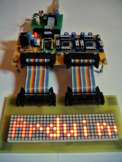
In order to provide a hardware reference for the Max696x Library for Arduino, I will describe the hardware platform I built for developing the MAX696x Library software.
I obtained some sample MAX6960 devices from Maxim and developed my own hardware based around two MAX6960 ICs and four red square 8×8 Led Matrices (LEDMS88R) from Futurlec.com.
The design I ended up with involved making 3 different boards:
- Interface Shield for Arduino
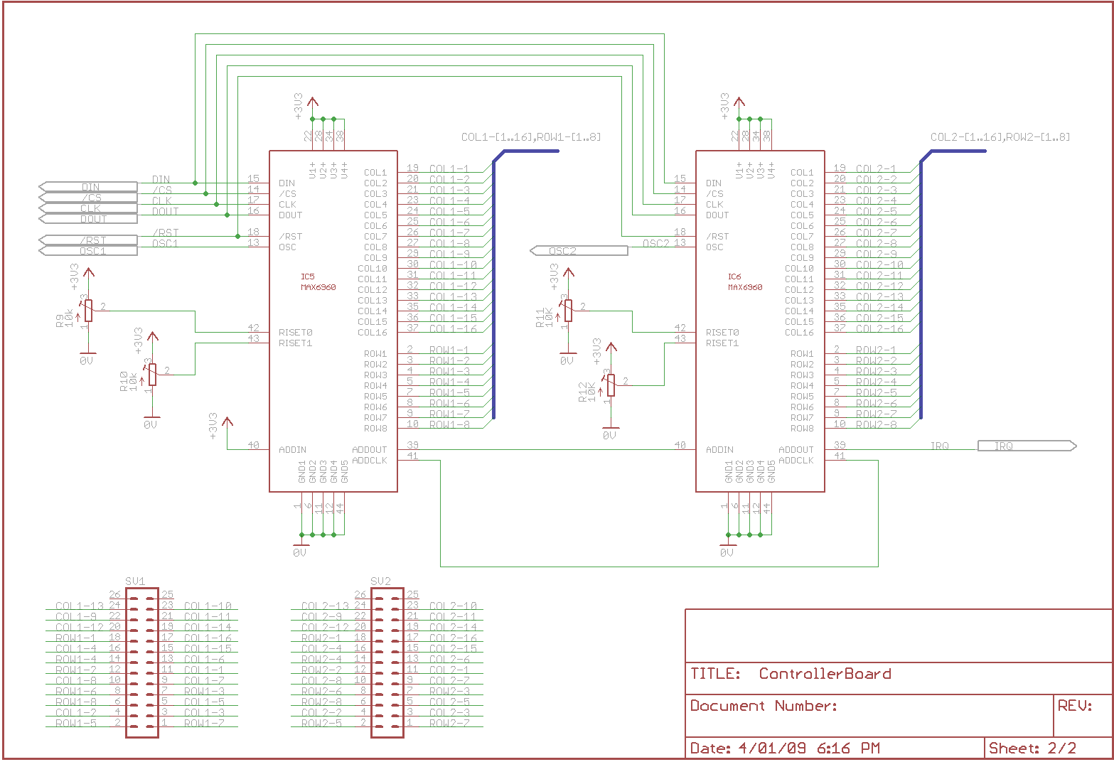
- MAX6960 Controller board
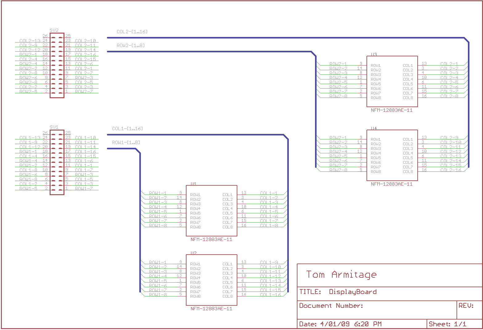
- Display board
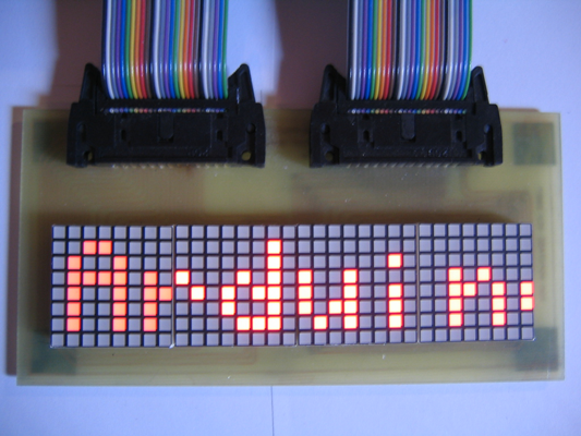
The result is shown in the following image:
Interface Shield
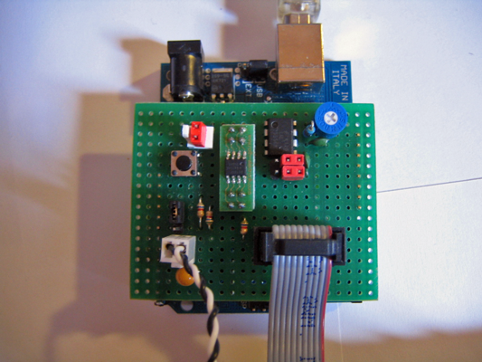
The Interface Shield connects the necessary Arduino pins to the MAX6960 Controller board. It brings power and control signals up from the Arduino board and provides connectors to interface to the rest of the circuit.
It’s major features are:
- 2-pin Polarised Power (PWR) Header (in white), to provide 5V to the MAX6960 Controller board.
- 10-pin Polarised Interface (I/F) Header (in black), to interface the Arduino signals to the MAX6960 Controller board.
- Reset button, to duplicate the Arduino Reset Button.
Interface Shield Schematic:
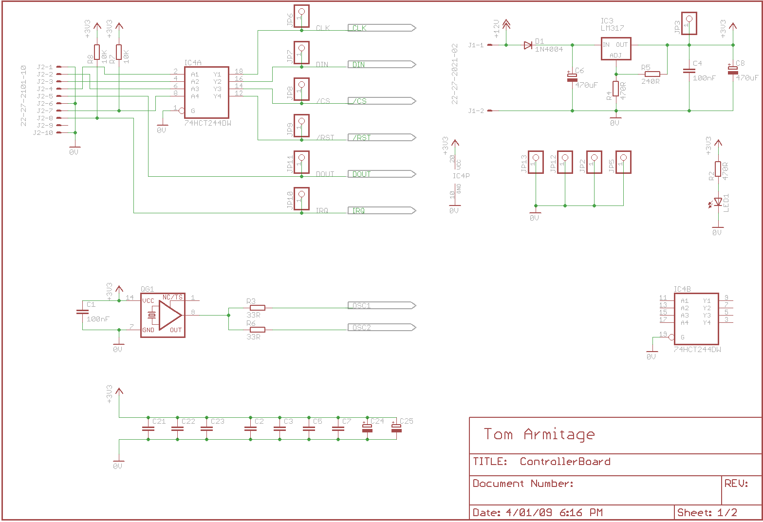
The Arduino has +5V available for circuits attached to the board, I decided to use this to power the MAX6960 Controller board using a 2-pin header on the shield connected to the Ardiuno POWER 5V and GND pins as shown:
| PWR Header Pin | Voltage | Arduino Pin |
|---|---|---|
| 1 | +5V | POWER 5V |
| 2 | GND | POWER GND |
I made the Interface Shield also able to select the Arduino VIN instead of +5V using jumpers so that I could use an external plug pack if required, but in the end it was not needed.
The MAX6960 devices use a 4-wire synchronous serial to communicate with the Arduino controller. This consists of a clock, a serial line in, a serial line out and a select line. The ATmega168 has a hardware SPI interface which are available on digital I/O pins on the Arduino board. I decided to the hardware SPI interface because using it makes the driver simpler. Instead of toggling all the bits manually in the code, the hardware SPI interface does all the hard work for you, and much faster to boot!
The Arduino hardware SPI interface is a synchronous serial interface and uses the following pins:
- DIGITAL 13 – SCK – Serial Clock – output from Arduino (ATmega168 pin 19). This is the clock of the serial interface and is generated by the Arduino board.
- DIGITAL 12 – MISO – Master In, Slave Out – input to Arduino (ATmega168 pin 18). As the name suggests, this is the serial data input to the Arduino, clocked in one bit at a time.
- DIGITAL 11 – MOSI – Master Out, Slave In – output from Arduino (ATmega168 pin 17). As the name suggests, this is the serial data output from the Arduino, clocked out one bit at a time.
- DIGITAL 10 – SS – Slave Select – output from Arduino (ATmega168 pin 16). This signal is used to address specific devices on the SPI bus and is driven low before any data transfer.
These are all standard synchronous SPI signal names, for more information I suggest reading the ATmega168 datasheet. These signals connect to the 10-pin Polarised header on the Interface Shield, along with a couple of connections to the Ardiuno GND.
Note that the MAX696x Library for Arduino can work without the hardware SPI interface. You can allocate the pins to any free digital I/O pins on the Arduino and use them instead, but there is a performance penalty in doing so because you will no longer be using the hardware SPI interface. To do this you will have to edit the library settings and recompile it.
The design I came up with requires 2 other signals and these also connect to the 10-pin Polarised Header on the Interface Shield and are:
- DIGITAL 9 – /RST – MAX6960 Controller Board Reset – output from Arduino (ATmega168 pin 15). This is an active low signal used to reset the MAX6960 devices on initialisation. The Arduino Reset circuit is not suitable because it does not meet the timing or voltage requirements of the MAX6960.
- DIGITAL 8 – IRQ – MAX6960 Controller Board Interrupt – input to Arduino (ATmega168 pin 14). This is signal allows the MAX6960 Controller Board to signal back to the Arduino that a memory plane change has occurred and that the memory in the MAX6960 display drivers can be updated.
I used the following pin out for the 10-pin Polarised header, noting that alternate names for each signal is given here in order to tie in with the schematic for the MAX6960 Controller Board:
| I/F Header Pin | Signal | Arduino Pin |
|---|---|---|
| 1 | GND – 0V | POWER GND |
| 2 | SS – /CS | DIGITAL 10 |
| 3 | MOSI – DIN | DIGITAL 11 |
| 4 | SCK – CLK | DIGITAL 13 |
| 5 | MISO – DOUT | DIGITAL 12 |
| 6 | GND – 0V | POWER GND |
| 7 | /RST | DIGITAL 9 |
| 8 | IRQ | DIGITAL 8 |
| 9 | Not Connected | N/A |
| 10 | GND – 0V | POWER GND |
Also seen on the Interface Shield is a DS1307 Real Time Clock IC (the 8-pin SMT device on the DIP adapter board), various jumpers, resistors and a 32kHz oscillator circuit based around a 555 Timer IC (the 8-pin DIP device). These are all superfluous to the operation of the Interface Shield and are not required. I added them so I could experiment with the I2C interface on the Arduino and change the supply voltage to the MAX6960 Controller board if needed.
The construction method I used is a simple one: single sided prototyping board with 0.1″ holes, cut to size. I used strips of standard single row 0.1″ male headers to connect to the Arduino and a combination of tinned copper wire and 30AWG kynar wire on the back of the board to make all the connections to the PWR and I/F headers. A similar prototyping board to the one I used is the Experimenters Board (EXPBRD) available from Futurelec.com.
Note that the SPI bus runs at high speed (8 or 16MHz) when using the hardware SPI interface. This means you should take care not to use longer wires than you need to (especially for SCK, MOSI and MISO) on your Interface Shield, keep cable lengths and return paths short and use decent power supply decoupling in your design.
Interface Shield Parts list:
MAX6960 Controller
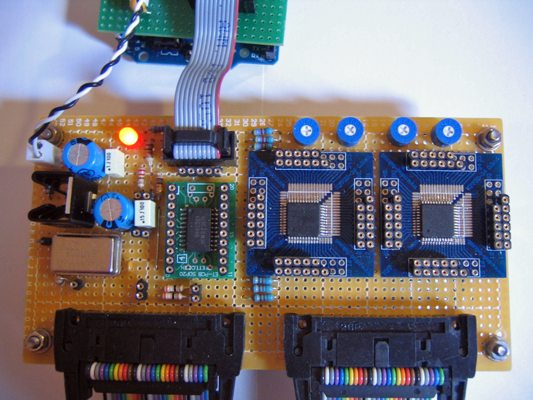
The controller consists of 3 separate parts:
- Power Supply
- Controller Interface and signal level shifting
- MAX6960 ICs, Clock and Display interface
The Power Supply converts the +5V from the Arduino to +3.3V required for the MAX6960 devices, in fact the +3.3V supply powers every device on the Controller board. The MAX6960 cannot be powered from +5V, if you connect it directly to the +5V supply, it will probably be destroyed.
The Controller Interface converts all the +5V digital signals (SPI bus signals and /RST) to +3.3V levels. As well as requiring a +3.3V power supply the MAX6960 cannot cope with +5V input signals. Directly connecting signals from the Arduino to the MAX6960 for more than a short while will destroy the MAX6960. I used a 74LVC244 dual quad buffer IC to convert the +5V signals to +3.3V levels. The LCV family of devices can operate on +3.3V power and handle with +5V inputs without blowing up.
MAX6960 Controller Schematic:
The power supply is required to generate a +3.3V supply for the rest of this board from the +5V supply
NOTE: If you are building your own display following this design you may need to use an external plug pack power supply and wire Arduino POWER VIN to PWR Header Pin 1 if you can’t find a low drop out +3.3V voltage regulator to use on your MAX6960 Controller board. In this case, a low drop out voltage regulator is one that will deliver +3.3V from a supply less than +4.3V, such as the National Semiconductor LM1117T-3.3. The voltage regulator should also be able to handle more than 500mA.
The MAX6960 is a 3.3V surface mount device. I used some QFP 32-64 0.5/0.8mm surface mount PCB adaptors from an eBay seller named mind-tek.
MAX6960 Controller Parts list:
Display
Display Schematic:
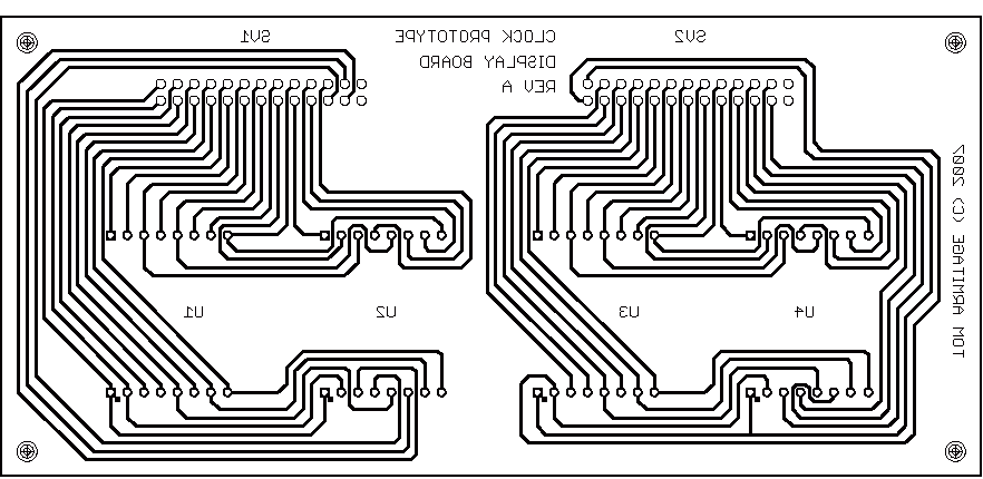
Display Layout:
Display Parts List:
this looks amazing!
could you please update which Clock Rate you used for the the Max6960?
It would be also very helpful, if you could post your arduino code for the scrolling text example!
thanks again!
At this stage I don’t have an example with scrolling text for the MAX6960 display driven from the Arduino. I have a font I will also post at some point and routines to convert strings to display data but not scrolling. Scrolling shouldn’t be too hard for you to work out.
The display I built uses a 8.10018 MHz oscillator module, it’s just what I had on hand at the time. If you use a different clock you need to change the frequency in the max6969x_conf.h file in the Library I posted. Then delete the .o file in the library directory and recompile your code.
The data sheet says that anything from 1MHz to 8.5MHz will do for a clock. The frequency you choose only effects the maximum and minimum frame rates if you operate in automatic memory plane switching mode. Just make sure you use a 3.3V clock.
I will eventually put up more detailed information about the display I built and better instructions about how to use the library… only so many hours in a day!
one question regarding daisy-chaining a couple of max6960. do you use your CMOS clock’s output to connect to all OSC inputs of the maxim chip or does each chip needs its own clock?
thanks so much!
I keep meaning to find the time to add more information to this page including schematics, parts lists etc.
The way I did the clock is like a kind of star arrangement with the CMOS oscillator module feeding two series termination resistors, ie about 33 ohm or so in series with each connection to a single MAX6960 from the oscillator, rather than daisy-chaining the clock from one MAC6960 to the next.
This is to try and keep the clock clean (ie prevent ringing etc). I initially ran the clock through two gates of a buffer IC to produce two individual clocks with series termination resistors, but my wire wrap construction technique wasn’t up to the job and it made all the other signals on the buffer IC noisy.
The termination resistors are to dampen any ringing on the line by trying to match the characteristic impedance of the clock signal wires. The value of 33 ohms is a best guess, anything from 22 to 100 ohm should work.
Don’t forget that the clock also has to be 3.3V for the MAX6960! I used a 5V part but found it worked ok at 3.3V.
According to the datasheet of the max6960 evkit (http://www.maxim-ic.com/quick_view2.cfm/qv_pk/5052) which hosts 4 max696x chips on one board (page 17), they have been using a 3state logic buffer for the output of the oscilator which connects to all other OSC inputs.
Your termination resistor contraption sounds interesting. Could you please provide a schematic? (ascii drawing is sufficient 🙂 ) are they just in series with the cable going from clock’s output to osc input?
Anyhow, my cable running from the oscillator output to the 2nd board is just 5cm long. Is that already enough for noisy oscillator lines? unfortunately, i don’t have an oscilloscope to dig more into it!
thanks for your help so far
I’ve uploaded some images of the schematic I used and this shows the clock circuit, see the post above.
The series termination resistors are there to try and match the characteristic impedance of the wires to stop reflections generated by the high frequency components of the clock signal. This will manifest itself as ringing. The resistor will damp this ringing, and should be located near the oscillator output.
5cm isn’t that long, one of my clock lines is probably close to double that. In the photo of the MAX6960 Controller board above the two termination resistors are the two 33 Ohm resistors just above the black connector on the bottom left of the board.
You need to make sure you have a good, short path (ie low inductance ground connection) for the clock signal and return current to flow in, ideally running right next to each other. Make sure your oscillator and MAX6960 devices are well decoupled (100nF capacitors on every VCC pin) and the addition of some bulk capacitance (a couple of ~10uF or so electrolytics or tantalums) across VCC can’t hurt either.
I got my circuit working on prototype board using mostly wire-wrap connections. The key is to keep your connections as short as possible and think about how the return current will flow through the ground connections and keep that path as short as possible too, within reason.
The important thing to remember with high speed digital design is that there are much higher frequency harmonics in the clock signal than just the fundamental clock frequency, and these are the ones that will cause you trouble.
And big current loops = big trouble, unless you are building an antenna!